
Intel Cyclone® V FPGAs and SoC FPGAs
Cyclone® V FPGAs have lower total power compared with the previous generation, efficient logic integration capabilities, integrated transceiver variants, and SoC FPGA variants with an ARM*-based hard processor system (HPS). The product family is recommended for Intel Edge-Centric applications and designs.
Choose from the following variants: Cyclone® V E FPGAs with logic only, Cyclone® V GX FPGAs with 3.125 Gbps transceivers, Cyclone® V GT FPGAs with 6.144 Gbps transceivers, Cyclone® V SE SoCs with ARM*-based hard processor system (HPS) and logic, Cyclone® V SX SoCs with ARM*-based HPS and 3.125 Gbps transceivers and Cyclone® V ST SoCs with ARM*-based HPS and 6.144 Gbps transceivers.
Cyclone® V FPGAs provide the industry's lowest system cost and power, along with performance levels that make the device family ideal for differentiating your high-volume applications. You'll get up to 40 percent lower total power compared with the previous generation, efficient logic integration capabilities, integrated transceiver variants, and SoC FPGA variants with an ARM*-based hard processor system (HPS).
Cyclone® V E FPGA
Optimized for lowest system cost and power for a wide spectrum of general logic and DSP applications.
Cyclone® V GX FPGA
Optimized for lowest cost and power for 614 Mbps to 3.125 Gbps transceiver applications.
Cyclone® V GT FPGA
FPGA industry’s lowest cost and power for 6.144 Gbps transceiver applications.
Cyclone® V SE FPGA
Integrated ARM* Cortex*-A9 MPCore* Processor System optimized for lowest system cost and power for a wide spectrum of general logic and DSP applications.
Cyclone® V SX FPGA
Integrated ARM* Cortex*-A9 MPCore* Processor System optimized for lowest cost and power for 614 Mbps to 3.125 Gbps transceiver applications.
Cyclone® V ST FPGA
Integrated ARM* Cortex*-A9 MPCore* Processor System - FPGA industry’s lowest cost and power for 6.144 Gbps transceiver applications.
Intel Cyclone® V FPGAs and SoC FPGAs Benefits:
Tailored for High-Volume, Cost-Sensitive Applications
With Cyclone® V FPGAs, you can get the power, cost, and performance levels you need for high-volume applications including protocol bridging, motor control drives, broadcast video converter and capture cards, and handheld devices. Learn more about the advantages of Cyclone® V FPGAs in a variety of market segments.
SoC FPGAs–Your Customizable ARM* Processor-Based SoC
SoC FPGAs let you reduce system power, system cost, and board space by integrating a HPS – consisting of processors, peripherals, and memory controller – with the FPGA fabric using a high-bandwidth interconnect backbone. The combination of the HPS with Intel's 28 nm low-power FPGA fabric provide the performance and ecosystem of an applications-class ARM* processor with the flexibility, low cost, and low power consumption of the Cyclone® V FPGAs.
Reducing Total System Cost Through Integration
Because Cyclone® V FPGAs integrate an abundance of hard intellectual property (IP) blocks, you can differentiate and do more with less overall system cost, power, and design time. Key hard IP blocks include the following:
- Hard memory controllers supporting 400 MHz DDR3 SDRAM with optional error correction code (ECC) support.
- PCI Express* (PCIe*) Gen2 with multifunction support.
- Variable-precision digital signal processing (DSP) blocks.
- HPS Dual-core ARM* Cortex*-A9 MPCore* processor.
Industry-Leading Low Power and Low System Cost
- Up to 40 percent lower total power compared with Cyclone® IV GX FPGAs.
- Lowest power serial transceivers with 88 mW maximum power consumption per channel at 5 Gbps.
- Over 4,000 MIPS (Dhrystones 2.1 benchmark) processing performance for under 1.8 W (for SoC FPGA).
- Lower power due to increased use of hard IP blocks.
Also lowering cost – the FPGAs require only two power regulator voltages and come in wire-bond packages with small form factor options.
ARM*-Based HPS
The Cyclone® V SoC FPGA HPS consists of a dual-core ARM* Cortex*-A9 MPCore* processor, a rich set of peripherals, and a multiport memory controller shared with logic in the FPGA, giving you the flexibility of programmable logic and the cost savings of hard intellectual property (IP) due to:
- Single- or dual-core processor with up to 925 MHz maximum frequency.
- Hardened embedded peripherals eliminate the need to implement these functions in programmable logic, leaving more FPGA resources for application-specific custom logic and reducing power consumption.
- Hardened multiport memory controller, shared by the processor and FPGA logic, supports DDR2, DDR3, and LPDDR2 devices with integrated error correction code (ECC) support for high-reliability and safety-critical applications.
High-Bandwidth Interconnect
High-throughput datapaths between the HPS and FPGA fabric provide interconnect performance not possible in two-chip solutions. This tight integration provides:
- Over 100 Gbps peak bandwidth.
- Integrated data coherency.
- Significant system power savings by eliminating the external I/O paths between the processor and the FPGA.
Flexible FPGA Fabric
The FPGA logic fabric lets you differentiate your system by implementing custom IP or off-the-shelf preconfigured IP from Intel or its partners into your designs. This allows you to:
- Adapt quickly to varying or changing interface and protocol standards.
- Add custom hardware in the FPGA to accelerate time-critical algorithms and create a compelling competitive edge.
- Quickly deploy a custom ARM* processor without the extensive design, verification, and non-recurring engineering (NRE) costs required in ASICs.
Architecture Matters
Because Cyclone® V SoC FPGAs integrate many hard IP blocks, you can lower your overall system cost, power, and design time. SoC FPGAs are more than the sum or their parts. How the processor and FPGA systems work together matters greatly to your system’s performance, reliability, and flexibility. Intel® SoC FPGAs are designed to:
- Preserve the flexibility of processor boot or FPGA configuration sequence, system response to processor reset, and independent memory interfaces of a two-chip solution.
- Maintain data integrity and reliability with integrated ECC.
- Protect DRAM memory shared by the processor and FPGA with an integrated memory protection unit.
- Enable system-level debug with Intel’s FPGA-adaptive debugging for unmatched visibility and control of the whole device.
Do you know more about Altera's product uses, technical documents, and solutions related to Cyclone® V FPGAs and SoC FPGAs? Then quickly get in touch with Altera (Intel) Distributor - NANHUANG!
 IC FPGA 696 I/O 1517HBGA
 IC FPGA 600 I/O 1760FBGA
 IC FPGA 327 I/O 484UBGA
 IC FPGA 98 I/O 144TQFP
 IC FPGA 416 I/O 896FBGA
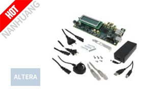 KIT STARTER CYCLONE IV GX
 IC SOC CORTEX-A9 1.5GHZ 1517FBGA
 IC FPGA 588 I/O 1517FCBGA
 IC FPGA 488 I/O 1152FBGA
 IC SOC CORTEX-A53 1.5GHZ 1760BGA
 IC FPGA 600 I/O 1152FBGA
 IC CPLD 440MC 5.4NS 256FBGA


- AMD-Xilinx Unlikely to Disrupt the Channel
- Altera Joins China Mobile R&D Program
- Altera & Wind River Deploy SoC Tools
- Altera and Intel Expand Fab Pact
- Altera Offers High-Efficiency Power Conversion for FPGAs
- Altera & TSMC Partner on Packaging
- Altera CEO Receives Semiconductor Industry Highest Honor
- Altera Debuts Nine New PowerSoC Devices
- Altera Dev Board Reduces Costs for Industrial Designs
- Altera Ships 20 nm SoCs
- Altera Design Doubles NAND Flash Life
- Intel Completes Acquisition of Altera
