

Altera Corporation (Intel) has developed a storage reference design, based on its Arria® 10 SoCs, that doubles the life of NAND flash and can increase the number of program-erase cycles by up to 7X compared to current NAND flash implementations. The reference design includes an Arria 10 SoC with an integrated dual-core ARM® Cortex®A9 processor, in an optimized, cost-effective, single-chip solution, leveraging a solid-state disk (SSD) controller from Mobiveil and NAND optimization software from NVMdurance. This reference design provides improved performance and flexibility in NAND utilization while reducing the cost of the NAND array by increasing the lifetime of data center equipment.
Using FPGAs with integrated hard processor systems, designers can quickly take advantage of the cost savings offered by next-generation NAND devices while retaining the flexibility to customize a solution that maximizes the performance, durability and storage capacity of their system. This storage solution implements Mobiveil’s Universal NVM Express Controller (UNEX), a configurable controller for PCIe-based SSDs, and NVMdurance’s NAND flash optimization software in an Arria 10 SoC, enabling data centers to leverage the most advanced 3D NAND technology without the long design cycles required with ASIC designs.
“An FPGA-based storage system provides hardware offload functions and makes specification updates easier to execute than flash storage designed with an ASIC SoC,” said Ravi Thummarukudy, CEO of Mobiveil Inc. “The new Arria 10 SoC—with its embedded ARM cores, PCI Express Gen3 and DDR4 interfaces—along with our SSD controller and IP from NVMdurance, squarely delivers what data center architects need in a NAND storage solution—improved power, scalability and total cost of ownership.”
In this reference design, Mobiveil’s controller supports multi-core architectures, enabling threads to run on each core with their own queue and interrupt without any locks required. NVMdurance’s NAND flash optimization software constantly monitors the condition of the NAND flash and automatically adjusts the control parameters in real time, greatly extending the flash system’s endurance. The Altera reference design also features end-to-end data protection, encryption and compression, and optimizes throughput and power consumption, all in a small silicon footprint.
“Until now, it was not possible to make the economics of FPGA flash storage work,” said Robert Pierce, senior marketing manager, compute and storage business unit, Altera. “Our Arria 10 SoC-based solution will make architects rethink how storage is deployed in the cloud and in high-performance computing systems—opening up new ways to innovate and extend a company’s investment, while providing the fast time-to-market that can be a competitive differentiator.”
All registered trademarks and other trademarks belong to their respective owners. For more details, please visit Altera (Intel) official site.
 IC SOC CORTEX-A9 925MHZ 896FBGA
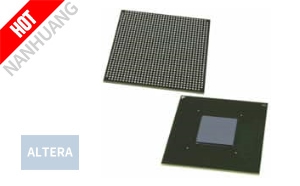 IC FPGA 544 I/O 1152FBGA
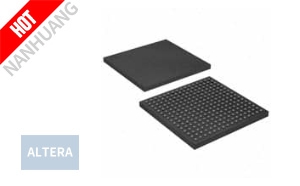 IC FPGA 171 I/O 256FBGA
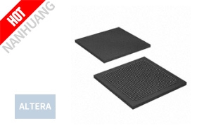 IC FPGA 613 I/O 780FBGA
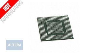 IC SOC CORTEX-A9 600MHZ 672UBGA
 IC FPGA 480 I/O 896FBGA
 IC CPLD 320MC 15NS 84PLCC
 MAX 10 FPGA 10M50 EVAL KIT
 IC FPGA 613 I/O 780FBGA
 IC CPLD 128MC 7.5NS 100TQFP
 IC CPLD 32MC 7.5NS 44PLCC
 IC FPGA 432 I/O 1152FBGA


- Intel Completes Acquisition of Altera
- Altera announced the first shipments of its 28 nm SoC devices
- Altera and Palmchip announced their partnership to provide the industry's first system-on-a programm
- Altera announced the first successful demonstration of the Suricata Engine
- Altera is demonstrating a new NAND Flash reference design that extends the life of flash memory up
- Altera announced its SDK for OpenCL is now included on the Khronos Group list of OpenCL conformant p
- Altera announced the latest release of the Altera SDK for OpenCL supports IBM Power Systems servers
- AMD-Xilinx Unlikely to Disrupt the Channel
- Altera Joins China Mobile R&D Program
- Altera & Wind River Deploy SoC Tools
- Altera and Intel Expand Fab Pact
- Altera Offers High-Efficiency Power Conversion for FPGAs
